EE171
EE171
Electrical Engineering Department
Portland State University
Portland, OR
MENTOR TOOLS TUTORIAL SESSION #2
Douglas V. Hall
Craig Files
Electrical Engineering Department
Portland State University
P.O Box 751
Portland OR, 97207
Version C2
September 1998
INTRODUCTION
In the first tutorial session you learned to invoke the
Design Manager environment, bring up the BOLD Browser, and use
basic window environment techniques to find a desired Mentor tool
manual. In this session you will learn how to use Design
Architect to draw and plot a simple schematic.
At the conclusion of this session you should be able to:
- Invoke Design Architect and set required options.
- Place a border and title block on a drawing
- Get and place library components.
- Select, copy, move, and delete components.
- Draw nets.
- Change names on input and output connectors.
- Check a sheet for errors.
- Save a sheet.
- Plot a sheet.
NOTES:
- means press the Return key on the keyboard.
- EXAMPLE DISPLAY - if you click on this link it will bring up an example
picture of the tutorial.
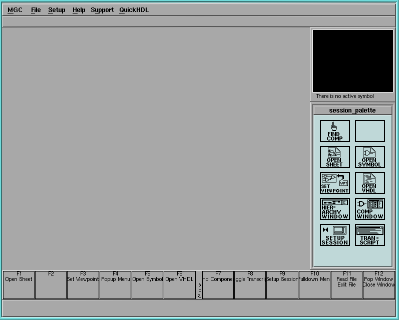
INVOKING DESIGN ARCHITECT
- Again, you must type in the following commands:
setenv MGC_WD /u/your_user_name
dmgr
- Once Design Manager is loaded, use the scroll arrows or elevator bar
to find the Design Architect icon (in the left window).
- Click the left mouse key on the icon to select it, press and
hold the right mouse key to bring up the Tool Operations menu, and
select Open. Alternatively, you can just double-click the left mouse
key on the Design Architect icon.
- When the Design Architect window appears, put the cursor on the
lower right corner of the window, hold down the left
mouse key, and drag the corner of the window down and to the right
until the window fills most of the screen, then release the mouse
key.
EXAMPLE DISPLAY
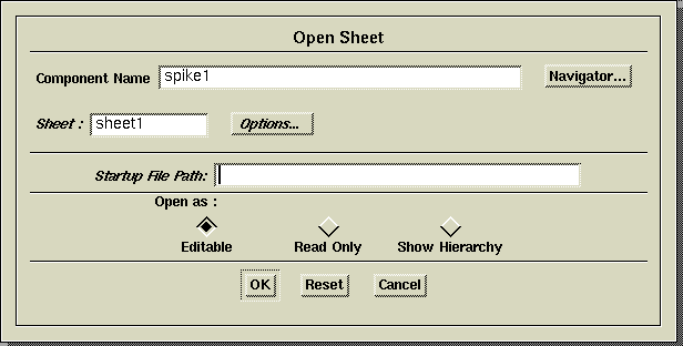
OPENING A SHEET AND SETTING GRID SPACING
- Click the left mouse key on the OPEN SHEET icon in the Session
_palette section of the Design Architect window.
- When the Open Sheet form appears, you want to enter a
Component Name which corresponds to the filename where you want
the schematic to be written. Type spike1 in the Component Name
box and click the left mouse key on the OK button.
EXAMPLE DISPLAY
- After a short pause, the schematic window should appear.
Maximize this schematic sheet window by clicking the left mouse
key on the larger of the two small boxes in the upper right corner
of the sheet window. Note that the name of the schematic sheet is
shown along the top of the sheet.
- In the schematic window you should see a grid of dots and plus
signs. With the default settings the plus signs mark off inches
and the dots mark off 0.25 inches. For the drawings you will be
doing it is much more convenient to have the dots spaced at 0.100
inch intervals. Two steps are needed to do this.
EXAMPLE DISPLAY
EXAMPLE DISPLAY
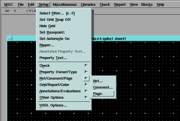
Put the cursor on the Setup entry along the top of the Design
Architect window, hold down the RIGHT mouse key, move the cursor
down to the Net/Comment/Page entry, then right and down to the
Page entry. Release the mouse key. When the Page form appears at
the bottom of the schematic window, move the cursor to the Pin
Space box and type 0.100, and then click the left mouse key on
the OK button.
EXAMPLE DISPLAY
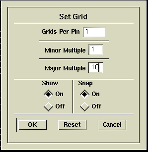
Put the cursor on the Setup entry again, hold the RIGHT mouse
key down, use the mouse to move the cursor down to the
Grid/Report/Color entry, then right and down to the Grid entry.
Release the mouse key. When the Set Grid form appears, put the
cursor in the Grids per Pin box and type 1. Move the cursor to
the Major Multiple box and type 10. Click the left mouse key on
the OK button. The spacing between the dots on the screen is now
0.100 inches.
EXAMPLE DISPLAY
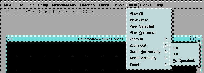
- The screen now only shows a small section of the sheet. To see
more of the sheet, use the RIGHT mouse key to pop up the View menu
at the top of the window, select Zoom Out, and release the mouse
key. Repeat the procedure to Zoom Out further. You should now see
that there are 10 spaces between each of the inch marks. If you
Zoom Out further, the 0.1 inch dots will disappear because the
resolution of the video display system is not great enough for
them to be visible with this view. Experiment the Zoom In and
Zoom Out commands to see their effects then stop with about 15
inches displayed horizontally.
- The hourglass shaped icon in the middle of the schematic
window represents the 0,0 coordinates for the schematic sheet.
Move the cursor around in the schematic window and you should see
the coordinates displayed above the upper right corner change as
you move the cursor.
- The next step is to show you how to move your view of the
sheet around. The best way to understand how this works is to
think that the entire schematic is pasted on the wall and that
you are looking at it through a hole in a movable piece of
cardboard. The arrows at the ends of the scroll bars along the
bottom and left side of the schematic window move your view hole
around. To see this, click the left mouse key on the arrow at the
left end of the scroll bar along the bottom of the screen. The
icon that was in the center of the screen appears to move to the
right, because you have moved you view hole to the left by
clicking on the left arrow. Play around with moving your view
until it becomes reasonably intuitive, then move the view until
the 0,0 icon is in the lower left corner of the screen.
ADDING A BORDER AND A TITLE BLOCK
- To make your schematic look sharp it is nice to put a border
around it. Borders, title boxes, and text added to a schematic
are referred to as comments. To add a rectangular border first
put the cursor on the Edit entry at the top of the screen, press
and hold the RIGHT mouse key, use the mouse to move the cursor
down to Edit Commands, right to Add Comment, and right to
Rectangle box, then release the mouse key. A plus shaped cursor
should appear.
Move the cursor to position (0.5,0.5), hold down the left
mouse key, use the mouse to move the upper right corner of the
box to coordinates (10.5,7.5), and release the mouse key.
- Use the process described in step 1 to add a 3.5 inch wide by
1 inch high title box in the lower right corner of the border.
Then use the Edit-> Edit Commands-> Add Comment->Line command to
draw a horizontal line across the center of the title box.
EXAMPLE DISPLAY
- Next you want to enlarge the view of the title block so you
can accurately enter a title and your name. Pop up the View
menu at the top of the window and choose View Area. When the
menu disappears, put the cursor just above and to the left of
the title block, hold down the left mouse key, and drag the
mouse down and to the right. When the view box encloses all
the title block, release the mouse key. The title block
should now fill the window. Note: To view the entire sheet
again, use the View->View All command from the banner View
menu.
- Now you want to put some text in the title block. Use the
Edit->Edit Commands->Add Comment->Text command to bring up the
Add Text form. Move the cursor to the form in the lower left
corner of the window and type SPIKE1. Then click the left
mouse key on the OK button. When your text appears, use the
mouse to move it to the center of the top box in your title
block, then click the left mouse key to place it.
- The default height for the text you inserted is quite small.
To change this to a more readable height, you use the Edit->
Edit Commands->Change Attributes->Text->Height command. When
the form for this command pops up, enter 0.2 as the text
height and click on the OK button.
- Use the process described in steps 4 and 5 to put your name
and date in the lower box of the title block.
MAKING A BACKUP COPY OF A SHEET
- About every 20 minutes you should save your schematic file so
that if something crashes, all is not lost. To do this put the
cursor on the File entry at the top of the Design Architect
window, hold down the RIGHT mouse key, move the cursor down to
Save Sheet and right to Default Registration, then release the
mouse key. At the bottom of the screen you will get a warning
that the sheet has not been checked but you can ignore this
warning. Eventually, at the bottom of the screen you will see a
message telling you that the file has been written and you can
proceed.
GETTING AND PLACING LIBRARY COMPONENTS
Now you finally get to draw a schematic. As a first example
you will redraw the circuit shown.
EXAMPLE DISPLAY
To reduce the amount of text you have to read from now on we
will use the following abbreviations:
- "click on" means "use the mouse to move the cursor
to the specified item, then click the left mouse key."
- "pop up the XXXX menu and choose the XXXX entry"
means "put the cursor in the indicated position, hold down the
right mouse key, move through the menu tree to the specified
choice as directed by ->, and release the mouse key."
For this schematic you will be using components from two
major libraries which are accessed through the Libraries entry
at the top of the Design Architect window. For logic devices
you will be using the models from Logic Modeling Corporation.
For Vcc, ground, portin, and portout connectors you will be
using the Mentor Graphics misc_lib. We will start with the
Logic Modeling Corporation components.
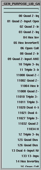
- Move the cursor to the Libraries entry at the top of the
Design Architect window, pop up the menu, and choose LMC
SmartModels. A list of the major LMC component sublibraries
should appear in a window on the right.
- After reading the available choices, click on the Gen Purpose
Logic entry. After reading the listing for the Gen Purpose
Library click on the Gate entry. When Gate listing appears,
click on TI. After a short pause the TI part list should
appear.
- Now, suppose you change your mind and decide that you really
want a Signetics part instead of a TI part. To go back to a
previous menu put the cursor in a blank section of the window
containing the list, With the right mouse key pop up and read
the Schematic Palette menu, then choose Back. This should take
you up one level in the menu tree. (If you want to go all the way
to the first menu (root), you can choose Root in the Schematic
Palette menu). After you see how this works go back to the TI
library listing.
- The 00 2-In NAND entry at the top of the TI list represents
all the TTL devices such as 74LS00, 74S00, etc. To help you move
through this list to find a desired component you need to add
some scroll bars which we showed you how to use in session 1. To
add scroll bars, pop up the Palette menu and choose Show Scroll Bars.
EXAMPLE DISPLAY
- The first component you need is a 74LS10 3-input NAND for the
output gate of the circuit in Figure 1. Click on the 10 3-in NAND
entry in the TI list to see the different 74X10 devices
available. At the bottom of the 10 list you should see a POS
entry for SN74LS10 and a NEG entry for a 74LS10. For this output
gate you want the bubbled input OR representation, so click on
the NEG entry, then move the cursor to the schematic window.
- After a short pause a ghost image of the device will appear on
the sheet. Use the mouse to move the image to coordinates
(7.0,4.4) and click the left mouse key to place the component in
that position. Note that the origin point for any symbol is the
lower left corner. Also note that the component outline is
dashed. This means that it is "selected." We'll tell you more
about this later.
- For the top 74LS10 in your schematic you want the positive
logic symbol. Click on the 74LS10(POS) entry to get a copy of
this component and place it at coordinates (5.2,5.4). Get another
positive 74LS10 and place it at coordinates (5.2,4.4).
- The next components you need are some 74LS00's. Use the
procedure described in 2 above to go back to the TI library
listing, then click on the 00 2-In NAND entry. Use the procedure
described in 4 and 5 above to get a POS 74LS00 and place it at
coordinates (5.2,3.3). Get each of the other three 74LS00's
needed for the circuit and place each in an appropriate
location.(Don't worry about exact placement, because in the next
section you will learn how to easily move components around on
the schematic.)
- You should now have all the logic devices on your schematic.
If you haven't remembered to do so, save your file as described
in the MAKING A BACKUP COPY OF A FILE section above.
- The next step is to add the portin, portout, and VCC
components to the drawing. As mentioned before, these components
are in the Mentor misc library. To get to this library, pop up
the Libraries menu in the top border and select MGC_Digital
Libraries. When the library list appears in the right window,
put the cursor in a blank section of the left window, pop up the
Palette menu, and add some scroll bars so you can easily move
through the list. Find the misc_lib entry in the list and
click on it.
- Click on the portout entry and move the cursor to the
schematic window. When the portout symbol appears, place it about
one inch to the right of the output of the circuit. Use the same
procedure to add the required portin connectors and Vcc symbols
to your schematic.
- Before we show you how to draw the nets(wires) required to
complete your schematic, we will show you how select, move,
copy, and delete components so you can reposition components if
necessary. Along the way we will also review how you can get an
expanded view of a specific area of your schematic. To get ready
for this, pop up the banner Edit menu, work your way to the
Unselect->All->Anything command, and release the mouse key.
VIEWING, SELECTING, COPYING, MOVING, AND DELETING COMPONENTS
- To more accurately place components you often want to expand
a section of the schematic. To do this, pop up the banner View
Menu, choose View Area, and release the mouse key.
- Move the cursor to a point just above and to the left of the
top 74LS10. Hold the left mouse key down and move the cursor down
and to the right until the displayed box contains just the three
74LS10's and the lower 74LS00, then release the left mouse key.
When you release the left mouse key, the enclosed area will be
expanded to fill the entire screen. Note: you can use the View->
View All command to see the entire sheet again.
- Now that you have the components placed on your schematic,
we need to introduce you to another set of command menus. To
access these menus, put the cursor in a blank area of the
Schematic window, and hold down the right mouse key. When a menu
appears, move the cursor to the Other Menus entry and then to the
right. After reading the list of six menus, move the cursor to
the Instance menu entry and release the mouse key. The Instance
menu should then appear. For future reference note the commands
available in this menu. To choose a command in one of these
menus, move the cursor to the desired command and click the left
mouse key. Exit the menu without executing a command by clicking
the left mouse key with the cursor anywhere outside the menu.
- The menu you have just seen allows you to copy, move, or
delete a component, but you must first select it.
One way to select a component is to place the cursor on the
component and click the left mouse key. The component outline
will become dashed to indicate the component is selected. A more
powerful way to select a component or group of components is to
pop up the Instance menu and choose Select-> Area. When the menus
disappear, move the cursor to a point above and to the left of
the area you want to select. Hold down the left mouse key, move
the mouse to create a box which contains the components you want
to select, and release the mouse key.
To unselect a component or components pop up the Instance
menu and choose Unselect -> All-> Anything.
After you unselect everything, use one of the above methods
to select the bottom 74LS00 in your schematic.
- To copy a selected component, pop up the Instance menu and
choose Copy -> Selected. When you move the mouse slightly, a
ghost image of the selected component will appear. Move the ghost
image an inch or so to the right and click the left mouse key to
place it there.
- Note that after you place a device, the device outline remains
dashed which means that it is still selected. You can pop up
the Instance menu and choose Move->Selected to move the device
around and just click the left mouse key to place it. Experiment
with moving the 74LS00 copy around.
- To delete a selected component, pop up the Instance menu and
choose Delete -> Selected. Use this procedure to delete the copy
of the 74LS00 you added to your schematic.
- If you accidentally delete a component, and you have not done
any other actions, you can undelete it by popping up the
Instance menu and choosing Undo. Use this technique to restore
the 74LS00 you just deleted. When you release the mouse key, the
deleted component should return, healthy as ever.
- Delete the extra 74LS00 again, before going on to the next
section.
DRAWING NETS (WIRES)
The next step is to draw some NETS or wires which connect
the gates together.
- With the cursor in the schematic window press the right mouse
key to pop up the ADD menu (if you cannot find it look under Other Menus).
In the Add menu choose Wire. When the menu disappears,
the cursor should change to a +.
- Move the + cursor to the diamond shaped box on the output of
the rightmost 74LS10, click the left mouse key, and move the
cursor to the right. A net should follow the cursor.
- Move the mouse to drag the end of the net to the diamond
shaped box on the left edge of the portout connector and quickly
click the left mouse button twice to end the net.
- Until you click on the cancel button at the bottom of the
Schematic window or Press the Esc key on the keyboard you are
still in net drawing mode, so you can draw another net.
Move the cursor to the diamond shaped box on the output of
the upper 74LS10 and click the left mouse key to start a net. Use
the mouse to drag the end of the net right to coordinates
(6.4,5.5), click the left mouse key to insert a turn, drag the
end of the net down to coordinates (6.4,4.6), click the left
mouse key to insert another turn, then drag the end of the net to
the top input of the output 74LS10. Terminate the net at that
point by double clicking the left mouse key.
- If you accidentally get a net that you don't want on the
drawing, you can delete it. First press the Esc key or click on
the Cancel button at the bottom of the Schematic window. Then pop
up the Instance menu and choose Unselect -> All -> Anything.
Next, select the net you want to delete by clicking on it.
Finally, pop up the Instance menu and choose Delete -> Selected.
- Draw additional nets required to complete your schematic.
(Remember, you can use the View All and the View Area entries in
the banner View menu to get a closeup view of different areas of
your schematic or you can use the scroll arrows and elevator bars
to move your view around on the schematic.
- Once you have finished drawing all the nets, click on the
cancel button at the bottom of the Schematic window to exit the
net editor.
- Pop up the banner View menu and choose View All so you
can look at you finished work.
- Use the banner File->Save Sheet command to make a
backup of your fine work.
CHANGING NAMES ON INPUT AND OUTPUT CONNECTORS
Note that the PORTIN and PORTOUT connectors are all
identified with the name NET. You need to change these names to
A, B, C, D, and Y as shown in Figure 1.
- Pop up the banner Edit-> Edit Commands -> Properties menu and
choose Change Text Values. When the Change Text Values form
appears, put the cursor in the Text Value box and type A.
Another box will appear under the A box. Move the cursor
into this box and type a B. Type a C in the third box, a D in the
fourth box, and a Y in the fifth box. This is all the names that
you have to change, so put the cursor in the OK box and click the
left mouse key. The form will then disappear.
- Place the cursor in the center of the NET label next to the
top PORTIN connector and click the left mouse key. An "A" should
replace the NET label. Place the cursor on the NET label next to
the portin connector second from the top and click the left mouse
key again. A "B" should replace the NET here. Repeat for the C
input connector, the D input connector and the Y output
connector.
CHECKING THE SHEET
Before you plot your schematic you need to check the sheet
and correct any errors found.
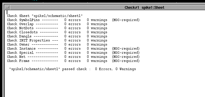
- To do this, pop up the banner Check menu and choose Sheet ->
With Defaults. When you release the mouse key, the circuit will
be automatically checked for wiring and other errors.
EXAMPLE DISPLAY
- If the report shows no errors, put the cursor in the little
box in the upper LEFT corner of the Report window, pop up the
menu there, and choose Close to get rid of the Report window.
If the report shows error(s), read the messages carefully
and think about what might be causing them. Then, to get the
Report window out of the way so you can correct the error(s),
click on the smaller of the two boxes in the upper RIGHT corner
of the Report window to iconize it for future reference.
(Remember, you can restore the Report window at any time by
putting the cursor on the icon, popping up the menu there, and
choosing Restore.)
- Fix any errors you found, save a copy of the corrected
schematic to a file, and check the sheet as described in step 1
above. Repeat steps 1-3 until the report shows no errors.
- Close any leftover Report windows.
PLOTTING THE SHEET
At this point you will send your plots to the one of the
laser printers. The available printers and their locations are as
follows.
    Printer

    lw7   (FAB CIRCUITS lab )
    lw10  (FAB SUN lab )
- Pop up the File menu at the top of the Design Architect
window and select Print Sheet.
EXAMPLE DISPLAY
- When the small form appears at the bottom of the Schematic
window, the default printer, enter the printer name and click on the OK
button.
- After some time your print should come out of the specified printer.
QUITTING DESIGN ARCHITECT.
- Save your sheet one more time to make sure the latest version
in on disk for future reference.
- Put the cursor in the banner at the very top of the Design
Architect window, pop up the menu there, and choose quit. After
a while the Design Architect window will disappear, but an
"orphan" command window will be left on the screen. To get rid
of this window, move the cursor into the window, hold the
Control key down and press the c key.
- To exit from Design Manager, put the cursor in the blank space at
the top of the window, pop up the menu there, choose Quit, and release
the mouse key.