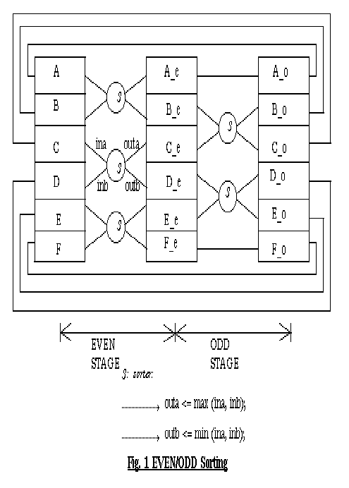
In this project, we design a sorter sorting a sequence of number using the
even/odd sorting algorithm shown in Fig. 1. During even sorting, data exchange
is only possible between two adjacent registers starting with even numbers.
Similarly, during odd sorting, sorting occurs between two adjacent registers
starting with odd numbers. After sufficient iteration (it's depend on the input
sequence pattern), all numbers are sorted.
2. Circuit Architecture and Design
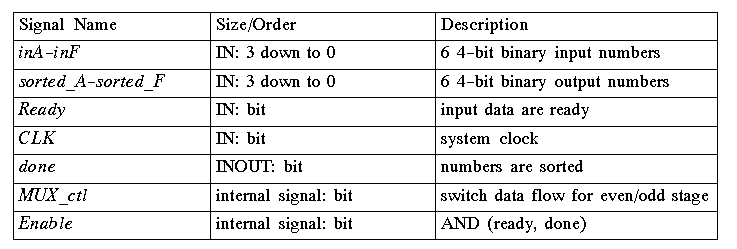
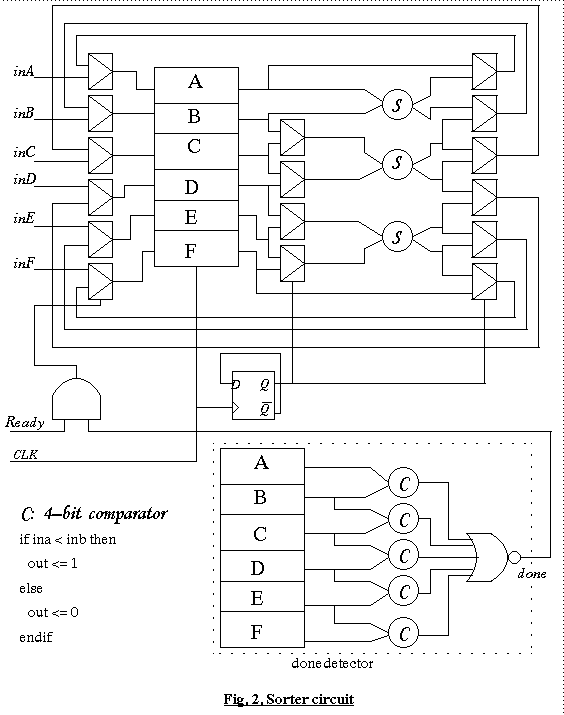
The circuit diagram is shown in Fig. 2. At this point we only use registers to represent data. (Later on we can implement in memory). Assuming we have 6 4-bit binary numbers, the 6 4-bit registers A-F are used to store the number. Following table lists the signal description.
The state machine design of this sorter is quite straight-forward. We use two
group multiplexers to switch the data flow for the even and odd stages. The
cycle time of the mux_ctl is 2x the clock period. The done signal detector is
composed of 5 4-bit comparators and a 5-input NOR gate, when all 6 numbers
are sorted, done raise to high. At the input of those 6 registers, we also
use a group of MUX to select between input signal and iterated internal results,
the control of this group of MUX is Enable=AND (ready, done), when both input
signals are ready and previous numbers are sorted, Enable raises and new group
of numbers are fed to registers and start sorting.
3. Simulation Results
Test 1
Test 2
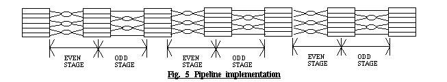
4. Pipeline expansion
This circuit is easily expanded to implement a pipeline structure shown in
Fig. 5. For the worst case, 6 stages are needed to get the final result. We
build all 6 stages such that after the initial pipeline latency, we can get
sorted results at the final stage each clock cycle.
Appendix A: VHDL Program Source Code
4-bit register
1-bit comparator
4-bit comparator
4-bit sorter
4-bit multiplexer
2-input nand gate
3-input nand gate
5-input nor gate
inverter