In this project, we implement a complete system to compute the Greatest Common Divisor(GCD) of the give two unsigned number using the
GLUSHKOV CONTROLLER model. In this system, control unit, memory and
data path are synchronized with one system clock, data and results are stored in memory,
it corresponds with ourter system with a system_start and a system_done signal.
It can be easily ported to any design needing a GCD. Simulation results
using Mentor Graphics VHDL tools are provided as well as the source code.
1. Algorithm description
The recursive algorithm for computing the GCD is:
BEGIN GCD(X, Y, Z)
IF (X = Y) THEN Z <= X;
END
ELSE
IF X>Y THEN
END IF;
S <= X-Y;
ELSE
GCD(Y, S, C);
R <= Y-X;
END IF;
GCD(X, R, C);
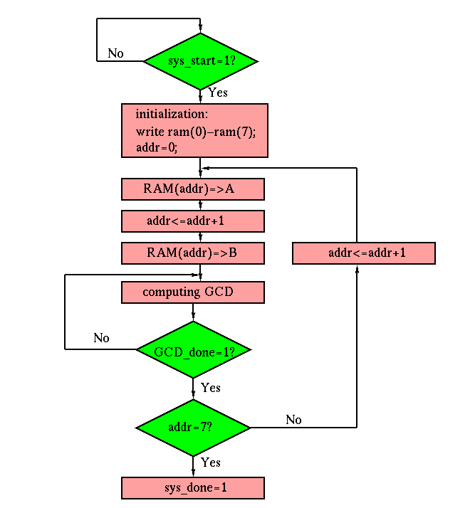
1. Computation flow chart
Assuming we have 4 pairs of unsigned numbers stored in 8 memory cells(addressed 0-7), upon system_start signal,
the GCD system compute the greatest common divisor for each pair of the numbers and
store the result back into the second cell. After all 4 pairs are calculated, the system_done
signal are raised high to imform that the computation is done.(just for practice.)
The flow chart for the circuit is shown in Fig. 1.
2. Circuit block diagram
The circuit is composed of 4 main components:


In order to implement the serial architecture of the GCD component, we use 3 8_bit registers A, B and C to store the two input number and the GCD result. We also need a comparator and a subtractor as well as multiplexers. At this point we built an adder_subtractor, and also use it as a comparator. Later on if want to optimize for speed or cost, we may consider to use faster comparator and subtractor. The block diagram for the GCD is shown below:

The 8 adder_subtactor is simply a ripple-carry adder, 8 1-bit full adders are cascaded to form the carry chain, Cin at the LSB select addition with subtraction. Cin control the selectionof addition with subtraction. the circuit are shown below:

Control Unit control the timing of the whole system. The timing is based on the computation flow chart. There are 7 control signals which consist different timing stages in the computation. They are:
| To GCD | To MEMORY | To Address Register | INPUT SIGNALS | OUTPUT SIGNALS |
| GCD_enA GCD_enB |
MEM_cs MEM_w/r MEM_do_init |
AR_reset, AR_inc | From system: sys_start, sys_clock From address register: addr_full Trom GCD: GCD_done | To system: sys_done |

With the state transition table:

The control unit is directly constructed from the state transition table. The address register is a 3-bit counter with AR_inc signal as the clock. The 3-bit address are connected to the memory which will decode the address to select a memory cell, and when Q0, Q1 Q2 are high, addr_full will be raised high and fed to the control unit.
1. Greatest Common Divisor Unit:

2. Memory Unit:

3. Address Register Unit:


At this point we don't do any optimization for this design(due to time limitation), but we can optimize for the following points:
1. optimize for speed.
2. optimize for cost.
3. optimize for area.
Appendix A: VHDL Program Source Code
Control Unit
a 8x8 RAM
3-bit address register
8-bit register
1-bit full adder
4-bit adder_subtractor
8-bit multiplexer array
all other small cells are availaber here!