PSU EE510VH Project 3-C
Automatic BIST Insertion to VHDL Code
June 12, 1998
Ram Koganti (rkoganti@ichips.intel.com)
Khader Mohammad (kmohamm@ichips.intel.com)
Dave McNeill (dmcneill@tqs.com)
Gerard Shaw (gerards@ichips.intel.com)
Class Presentation on BIST (in powerpoint)
Mentor Graphics Tool Suite Usage
This report describes the use the Mentor Graphics tool set for automatically inserting BIST code into VHDL code. For this project, BIST code will be instead into our code for the implementation of the Greatest Common Divisor algorithm. Included in this report is a brief introduction of BIST and a tutorial explaining the steps necessary to insert BIST code into a VHDL based circuit with the Mentor Graphics DFT tool suite.
This report is organized as follows. First, we describe some of the general acronyms used throughout the report. In section 2, we discuss why testing is important. Section 3 describes what BIST is. In Section 4, we present a tutorial on using Mentor BIST and Boundary Scan tools. In Section 5, we present our conclusions.
ATPG - Automatic Test Pattern Generator
CRC - Cyclic Redundancy Checking
CUT - Circuit (Component) Under Test
DFT - Design For Test
DUT - Design Under Test
BIST - Built In Self Test
JTAG - Joint Test Action Group
LFSR - Linear Feedback Shift Register
MISR - Multiple Input Signature Register
PSPG - Pseudo Random Pattern Generator
TAP - Test Access Port
UUT - Unit Under Test
Controllability - a testability metric that measures the difficulty in driving a node to a specific value. Example: driving '1' to an AND gate output.
Observability - a testability metric that measures the difficulty in propagating the value on a node to a primary output. Example: observing '0' on an OR gate input
Full Scan - all storage elements in the design are replaced by their scannbale equivalents.
Partial Scan - only a percentage of the storage elements are replaced.
Both methods increase the controllability and observability of the circuit.
Scan Cell - a basic independently accessible (controllable/observable) unit in the scan circuitry.
Scan Chains - a set of scan cells that have been serially linked together. Each scan chain contains an external input pin an external output pin that provides access to the scan cells.
Boundary Scan (IEEE 1149.1) - Design for Test (DFT) technique whose primary purpose is to facilitate the testing of printed circuit board (PCB) interconnect circuitry. On a PCB board, the input and output ports of the IC's it contains are stitched toge ther into a long scan path Provides an optional command "RUNBIST" than can be used to enable the self test within the IC.
Microelectronics is synonymous with making products smaller, faster, and denser. Functionality that 10 to 20 years ago now literally fits in the palm of your hand. Today's designers using Design Automation (DA) with the latest semiconductor tech nology are accelerating this rate of integration even more. This combination of increased functionality with the faster, denser, and smaller packaging brings up a dilemma: it is becoming more difficult to access, test, and verify chip and system functiona lity using traditional external equipment and instruments.
The automatic semiconductor test equipment has not completely been able to follow the semiconductor applications trend from large centralized mainframes to desktop or portable installations. Even the advanced testing equipment has mainframe-sized cabin ets for the tester electronics which connect to a device many orders of magnitude smaller. Testing equipment manufacturers have been exploiting the same integration density that they are trying to test. However, high operating frequency, high pin count, a nd high gate count create extremely complex electromechanical interfaces between the automatic tester and the unit under test. The test equipment manufacturers are dealing with a double-edged sword. The complex interface combined with the market demand fo r speed, flexibility, and accuracy push steeper requirements back onto the test equipment manufacturers. Given the time needed for developing and creating such complex equipment, the semiconductor products under test are usually more advanced than the tec hnology used in the tester electronics. Some of these problems can be addressed by using a technology called BIST.
BIST, which stands for Built-In Self-Test, approaches the problem from a different angle. BIST attempts to move as much of the tester functionality as possible onto the silicon. Embedding the tester equipment functionality into the semiconductor product not only reduces the burden on and the complexity of external test equipment, but the on-chip access is simplistic and faster. BIST is extra circuitry to enable complete testing without much external help. It basically consists of a test pattern generator, test response compactor, test response comparator, and control circuitry to carry out the test process and give the GO/NOGO signal. BIST is not a replacement for scan and does not result in fewer test patterns. BIST enabled designs still requir e the use of testers for certain portions of the design that BIST cannot be inserted.
BIST is the circuitry that enables a chip to test itself, and it has been consider as a good substitute for the ATPG(Automatic Test Pattern Generation) procedure which deterministically uses some algorithms to produce the funct ion vectors and their corresponding responses required for testers.
The main advantage of using BIST are: (i) eliminating (or at least minimizing) the costs of ATPG and fault simulations, (ii) shortening the time duration of tests (by running tests at circuit speeds), (iii) simplifying the external test equipment, and (iv) easily adopting to engineering changes. (in other words, low technology dependency.)
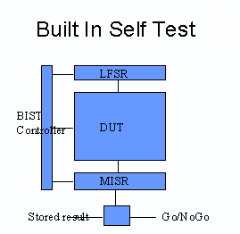
A simple BIST configuration, as shown in Figure 1, includes an LFSR (Linear Feedback Shift Register), and MISR(Multiple Input Signature Register), and some control circuitry. The LFSR basically produce pseudorandom input vectors, so it’s also called a PRPG (Pseudo Random Pattern Generator); the MISR (another type of LFSR) com-presses the response of the CUT(Circuit Under Test) into a signature to be compared to a good circuit’s response. The BIST results, "pass" or "fail", depend o n whether the signature captured into the MISR matches the one coming out of the good (golden) circuit.
Figure 1.
BIST insertion procedure using Mentor Tools consists of the following steps.
The Mentor Tools required for this tutorial are:
All these tools are available in the Mentor.B.4 tool suite installed on PSU Sun machines. To install this tool suite use the addpkg command. You can uninstall the tool suite by using the delpkg command.
Before you use the test and synthesis tools, create a directory where you will be executing the tutorial commands, and setup the following MENTOR envirnoment variables.
The $MGC_SYNLIB variable points to a CMOSN technology library which can used as the target for synthesis and optimization.
Before trying to insert full scan and BIST, please ensure that your RTL design satisfies the following design rules.
In this tutorial we will insert BIST and Boundary Scan into an RTL description of an algorithm that computes the Greatest Common Divisor of two unsigned 8-bit integers. Click here for the VHDL code.
Before proceeding with BIST insertion, we need to insert scan cells into the design. Scan cell improve the controllability and observability of the Circuit. Since BIST uses pseudo random test patterns, it is very hard to obtain good fault coverage without inserting scan chains into the design. Also, all the state elements in the design should have known values, if the BIST signature comparision is to work correctly. Using Full Scan will solve both these problems.
A netlist is necessary before FULL SCAN can be inserted into the design, using DFTAdvisor. In this section, we describe the procedure that can used the generate a netlist from the RTL description of the GCD circuit.
The GCD RTL description used a library called work to store all modular entities. Execute the following commands to create this library.
The next step is to compile the source code.
Use the -help option with alcom command to get a description of the different switches.
Once the souce code is compiled successfully, invoke autologic in the shell mode. In our session we be using the cmosn/1.2_worst technology defined in the $MGC_SYNLIB directory, as the target technology.
Within the autlogic shell execute the following commands.
Optimize each module in the GCD circuit one by one. There are four modules in the design, aminusb with an architecture named structural, acomb with an architecture named structural, mux8_2 with an architecture named structural and rst_e_reg8 with an architecture named dataflow.
Optimize the highest level entity (The GCD entity in this case).
The opt command produces a netlist. Save this netlist in both genie and vhdl formats.
The outputs from the above steps are two files, one is the netlist described in the GENIE format (gcd_comp.gn) and the other is a netlist described using structural VHDL (gcd_comp.vhd).
To insert full scan, we need to replace, all memory elements with scannable equivalents. This can be done automatically using DFTAdvisor. DFTAdvisor needs two input files to do this, one is a netlist and the other is an ATPG library that describes available scan cells and mappings between non-scan cells and equivalent scan cells.
The netlist we are going to use is the netlist generated by autologic in the previous stage. The ATPG library available along with the cmosn technology in $MGC_SYNLIB was outdatated and had compilation problems. Therefore we had to edit the library file. The editied library file can be found here (atglib).
The following commands should be executed to insert full scan into the netlist.
Invoke DFTAdvisor
Within the DFTAdvisor Shell, there are two modes, SETUP and DFT. SETUP mode is used to setup the scan insertion process, where as DFT is used to acturally insert the scan cells.
The following commands identify technology cells that DFTAdvisor can use in synthesizing the test logic.
Identify the clock. Currently DFT advisor supports only one primary clock.
Change to DFT System mode.
This command forces DFTAdvisor to do Full Scan.
Identifies the pin name that controls the inserted scan chains. In this case, the pin is name as scan_en.
Insert the scan chains. The -max_length flag specifies the maximum lenght of a single scan chain.
Save the scan inserted netlist in genie and vhdl formats. You can look at the output VHDL code and see that the entity description has been modified.
Save the ATPG setup files. This file provides scan chain information to downstream tools.
The above procedure produces four files, gcd_scan.gn, gcd_scan.vhd, gcd_scan.dofile and gcd_scan.testproc. gcd_scan.gn and gcd_scan.vhd are netlist descriptions of the scan inserted logic and gcd_scan.dofile is a mentor script that provides scan information for other tools.
BIST by its very nature, requires a large number of test vectors to achieve a high fault coverage. Many nodes are hard to control/observe with random input patterns. This problem is called Random Pattern Resistance. To provide an effective BIST solution, the circuit under test needs to be anlayzed to identify these hard to control/observe nodes and additional test logic (scan cells etc.) has to added to address this problem. Both these tasks can be done automatically by DFTAdvisor.
In Simulation based Test Point Analysis, DFTAdvisor uses fault simulation with a Random Pattern Generator to get an idea of the controllability/observability of all nodes. If nodes do not cross a user-specified "detection threshold" then a new scan cell will be created to control/observe a node. All newly created scan cells are stitched to form a new scan chain.
Invoke DFTAdvisor on the netlist with full scan. The inputs to DFTAdvisor for doing test point analysis are the full scan inserted component netlist and the ATPG library of the target technology.
Identify technology cells that DFTAdvisor can use in synthesizing the test logic.
Identify the scan chains and attributes. To identifiy the scan chains we will use the ATPG setup file produced in the previous stage, gcd_scan.dofile.
Specify the clock signal that will be used to control the scan chain.
The next step is to specify the Linear Feedback Shift Register (LFSR) and Multiple Input Signature Register (MISR) that will be used to apply test patterns and obsever nodes. These are for simulation purpose only, but to get the best analysis, it is preferable that their configuration be similar to the LFSR and MISR that will used in the final BIST inserted design. For convenience, the LFSR definitions, configuration and connections to internal nodes have been put in the Mentor script lfsr_defines.do. Execute the script using the following command.
Now, put DFTAdvisor in test_point analysis mode using the following command.
You also need to establish the criteria that DFTAdvisor uses to determine if a node has adequate controllability/observability. This can be done using the following commands. If during fault simulation, DFT Advisor finds that the value on a node can not changed or observed more than the threhold (5 in this case) number of times, it inserts a test point to control/observe that node.
Next, setup DFTAdvisor for Test Point insertion, by providing different parameters. The -control flag used to specify the maximum number of scan cells that can be inserted to improve controllability of the circuit. The -observe flag has a similar function. The -patterns flag specifies the number of input test patterns. The -base switch identifies the type of test point insertion to be done either simulation or multiphase test point analysis.
Limit the fault universe, by removing faults inside the basic components of the technology library.
Since Setup is completed, change the mode to DFT.
Identify the pin that will be used to enable the newly inserted scan chain. This pin should be the same as the scan_enable pin used to control the other scan chains, that were created when FULL SCAN was inserted into the design.
Identify the pin that will be used to insert serial data into into the new scan chain, and a pin to observe the outputs of the new scan chain.
Save the new netlist in genie and vhdl formats. Look at gcd_scan_tp.vhd to identify any extra interace and logic added.
DFTAdvisor also generates the script files that automate the task of inserting BIST into the netlist produced, and a high level entity that is required by the LBIST Architect.
The outputs of this stage are
Before proceeding with BIST insertion, the bist.dofile.old created in the last stage should be edited. Replace -clock <null> with -clock clk. Click here for the new bist.dofile.
To generate the BIST rtl around the core netlist, execute the following command. The inputs to LBIST architect are the BIST entity and the edited dofile, created in the last stage.
The outputs generated by this process are
Mentor BSDArchitect can be used to synthesize Boundary Scan as well as the TAP controller. BIST can be invoked by external tester via the IEEE 1149.1 interface using the RUNBIST instruction of the TAP controller.
To synthesize the Boundary Scan Circuitry, LBIST architect requires a map file bsda.map which provids a pointer to some vhdl files required by Mentor.
Generate Boundary Scan RTL description using the following command. The inputs to this phase are bsda_in.vhd and gcd_comp_bsda.do produced by LBIST architect during BIST synthesis.
The outputs generated by this process are
The outputs of the previous stages, gcd_scan_tp.gn (core netlist with scan and test points), bsda_in_umap.vhd (boundary scan circuitry) and gcd_comp_bist.vhd (BIST description) need to be linked and synthesized to obtain the final netlist.
To synthesize the top level circuit, we also need some mentor internal vhdl files, funcs.vhd, defs.vhd and bscmp.hdl.
The vhdl file bsda_in_umap.vhd requires a library mgc_bscan that is generated from the file bscmp.hdl. The vhdl file gcd_comp_bist requires the library mgc_hls, that is generated from the files func.vhd and defs.vhd.
The following text goes through the procedure for synthesizing all the files together.
Create and map the mgc_bscan library
Compile bscmp.hdl into the mgc_bscan library
Create and map the mgc_hls library
Compile funcs.vhd and defs.vhd into the mgc_hls library
Create a work library where the top level netlist will be assembled.
Compile the BIST and Boundary Scan RTL.
Synthesize the top level component.
Unfortunately at this stage, we were unable to link the three components together. As a result we could not synthsize the top level circuit.
Run FastScan on the top level netlist produced in the previous stage, to obtain the fault coverage of the BIST design and the good signature.
BIST is a DFT construct that is used for random logic as well as memory testing. In a BIST environment, Pseudo-Random(PR) test sets are used. BIST is an attractive test solution because it involves the implementation of testing hardware on-chip. In addition, it addresses challenges in the areas of at-speed testing and core testability.
Mentor BIST and Boundary Scan tools can speed up the process of designing BIST circuitry. The tools can be used to generates synthesizable RTL description of BIST and Boundary Scan circuitry. Mentor tools provide a new patented multiphase test point insertion (MTPI) methodology that can increase fault coverage of the BIST design. The BIST tools are integrated with DFTAdvisor to provide design rule checking, deterministic fault simulation, and MISR signature calculation. The BIST tools are also integrated with BSDArchitect to automatically generate IEEE 1149.1 control circuitry.
In our project we have successfully used Mentor tools to insert full scan into a GCD circuit. We also did Fault simulation based test point analysis and injected new test points into the design. We observed that Mentor multiphase test point insertion methodology does not support mux primitives. This could be be a serious problem, as very few practical designs do not use muxes. We also successfully used Mentor tools to generate BIST and Boundary Scan circuitry.
We failed to synthesize the top level netlist that included all the logic including the core netlist, BIST circuitry and Boundary scan circuitry. Though we used bold_browser instructions to link unmapped instances manually, the command did not succeed and we were unable to debug the reason (whether there was some problem in the files or whether it was a methodology issue.). Since we could not generate the top level netlist, we could not run fastscan to determine fault coverage and generate the good signature.
We had many problems during the project, including environment issues, segmentation faults on some machines and licensing problems. The biggest problems however were the lack of an expert user of these tools and poor documentation. The tutorials povided in the manuals did not include a tutorial to synthesize the top level netlist, which is where we got stuck. Overall the project was useful because we understood ATPG/SCAN/BIST/Boundary Scan and Mentor Tool Usage. Hopefully this tutorial will be useful to future users of the tool set.